|
|
|
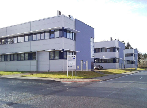
Electron Microscopy Group in
Material and Technologies department of
New Technologies Research Centre (NTC) belong to
University of West Bohemia (UWB) located in beautiful city
Pilsen.
You can download in
 or
or
 our department booklet.
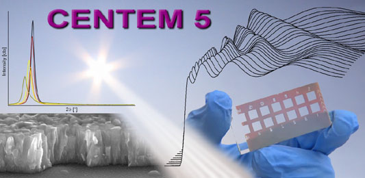
Department of materials and technology is in European
Union project (section 5 of
CENTEM) focused on basic research of new materials used for II. and III. generation thin films solar
cells. We deposit and characterize thin film ZnO, amorphous silicon,
microcrystaline silicon and silicon quantum dots for implementation as active material
in thin film silicon solar cells.
|
Microscopic laboratories
Transmission electron microscopy
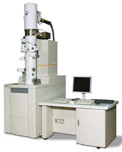 |
JEOL JEM 2200FS
- Field Emission (Schottky) electron gun
- Accelerating voltage: 80 – 200 kV
- Resolution 0.19 nm
- In-column energy filter (Ω-filter) for EELS analysis and
energy filtered imaging
- High-contrast imaging
- STEM mode
- EDS detector from Oxford
- 3D tomography reconstruction of samples
- Magnification
- TEM mode 50 to 1 500 000x
- STEM mode 100x to 150 000 000x
|
Scanning electron microscopy
 |
 |
|
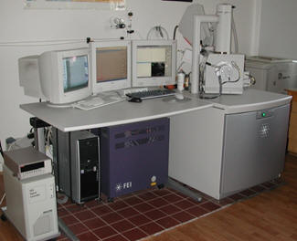
FEI Quanta 200
|
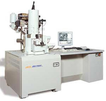
JEOL JSM 7600F
|
- High-performance thermal emission SEM with EDS
and WDS (microprobe) from EDAX
- Resolution
- High-vacuum
- 3.0 nm at 30 kV (SE)
- 4.0 nm at 30 kV (BSE)
- 10 nm at 3 kV (SE)
- Environmental mode (ESEM) for nonconductive samples without coatings
- Accelerating voltage: 200 V – 30 kV
- Probe current: up to 2 μA – continuously adjustable
|
- Field Emission (Schottky) for ultra-high resolution
- Gentle Beam (GB mode) to reduce damage of sensitive samples and reduce
charging of non-conductive samples
- Resolution
- 1 nm at 15kV
- 1.5 nm at 1kV in GB mode
- Element detectors EDS, WDS (microprobe) from Oxford
- Electron microdiffraction detector (EBSD)
- Build-in energy filter (r-filter) of measured electrons
- Magnification 25 – 1 000 000x
- Accelerating voltage: 100 V – 30 kV
|
Other Material and Technology Department laboratories
Thin film deposition
 |
 |
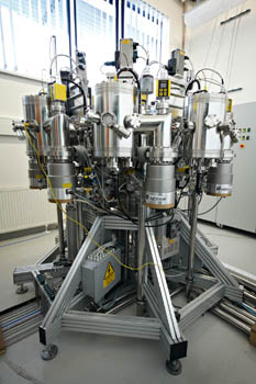 |
|
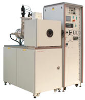
BOC Edwards TF600 electron beam evaporation and sputtering system
|
SAMCO PD 220NA
PE-CVD system
|
Elettrorava PE-CVD 5-chamber deposition system
|
- Deposition of thin films using PVD technology
- RF Sputtering – up to 600 W
- DC Sputtering – up to 1,5 kW
- Electron beam evaporation processing
- Automatic process control
- Turbomolecular and dry rotary pumping system
- Ultimate pressure: 4,35 x 10⁻⁷ mbar
- Process gas: Argon
- Working gas: Nitrogen, Oxygen
|
- Deposition of silicon oxide (SiOx)
- Deposition of silicon nitride (SixNy)
- Deposition of silicon oxy-nitride (SiOxNy)
- Deposition of hydrogenated amorphous silicon (a-Si:H)
- Fully automatic "one-button" operation time with full manual
override
- Homogeneous deposition area up to 300 mm
|
- Grow of thin film solar cell based on silicon in p-i-n / n-i-p configuration
- Deposition of silicon oxide (SiOx), silicon nitride (SixNy) and
silicon oxo-nitrides (SiOxNy) with refractive index and
semiconductor band-gap control
- Silicon doping to p- and n- conductivity type
- Simple and tandems structures, substrate / superstrate, micromorph
|
Optical spectroscopy
 |
 |
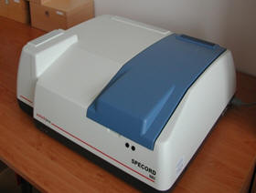
|
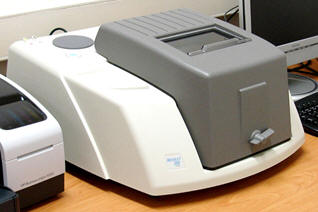
UV/VIS Spectrophotometer Specord 210 BU
|
Spectroscopic ellipsometer SENTECH SE850
|
- Spectral range 190 – 1100 nm
- Measurement of transmittance, absorbance and reflectance in
dependence on the wavelength
Possibility of optical parameters determination
- Thin film thickness measurement
- Spectral refractive index and extinction coefficient
- Dielectric functions
- Optical band gap in transparent semiconductors
|
- Spectral range 240 – 2500 nm
- Ellipsometric parameters ψ, ∆, transmittance and reflectance
measurement in dependence on the wavelength
Possibility of determination parameters of individual thin
layers
- Thin film thickness and surface roughness
- Optical properties
- Spectral refractive index and extinction coefficient
- Dielectric functions
- Optical thickness of band gap in transparent semiconductors
- Electrical properties
- Resistivity, concentration and mobility of charge carriers
|
Vibration spectroscopy
 |
 |
|
FTIR Spectrometer NICOLET 380
|
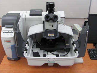
DXR Raman Microscopy
|
- Max / min range limit 7800 – 350 cm –1
- Measurement of transmittance, absorbance and
reflectance in dependence on the wavenumber
Accessories
- Specular Reflection Accessory (for surface analysis)
- Smart SAGA (for the analysis of thin films on reflective
substrates, the 80 degree angle of incidence, sensitive
measurement of films as thin as 0.1 nm)
- iTR Ge attachment with reflectance amplification effect in range
4000 – 400 cm-1
|
- Spectral range 3000 – 50 cm-1
- 4 excitation lasers (532 nm, 633 nm, 780 nm high-performance,
780 nm high-luminance), motorized table with 3-axis movements
- Microscope have trinocular for visual view and
video-screen simultaneously
- Head can carry 5 objectives – 4x, 10x, 20x, 50x,
100x with long working distance
Possibilities of Raman spectroscopy
- Identification of chemical compounds
- Homogeneity of structure
- Polymers and biopolymers application
- Pharmaceutics application
- Mineralogy, authenticity and quality of rare minerals
- Control of raw materials
- Art and archeology
|
X-Ray diffraction
 |
 |
|
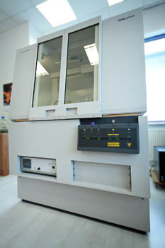
Automatic diffractometer Panalytical X’Pert Pro
|
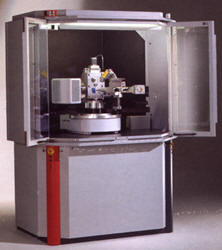
Automatic diffractometer Bruker AXS D8 Discover with 2D detector
|
|
Applications:
- Qualitative and quantitative phase analysis
- Residual stress analysis
- Texture analysis
- Analysis of changes in the crystal structure
- High temperature phase transformations
- Ultra fast data collection with X’Celerator
- Thin film analysis – signal measured from thin film only without
influence of signal from substrate – Xe detector (primary
monochromator possible)
- Can be used for bulk materials, powders and thin films
|
Measurement possibilities:
- Qualitative and quantitative phase analysis
- Qualitative and quantitative texture analysis
- Residual stress analysis (lattice stress)
- Microstructure (microstrain, crystallite size)
|
Optical microscopy
 |
 |
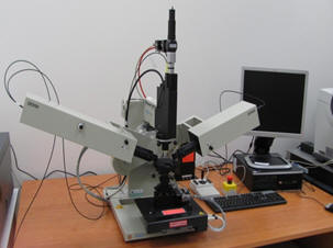
|
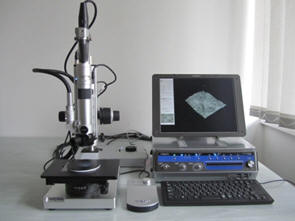
3D digital optical microscope HIROX KH 7700
|
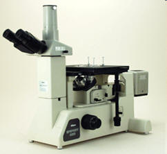
Metallographic microscope Epiphot 200
|
- Magnification range 5 - 3 500 x
- High depth of field
- Dimensional and shape measurement
- Evaluation of 3D profiles
- Possibility of big parts evaluation
|
- Magnification 50x – 1000x
- Brightfield observation
- Darkfield observation
- Simple polarization observation
- Nomarski DIC
|
Thin films profilometry, resistivity and efficiency measurement
 |
 |
 |
|
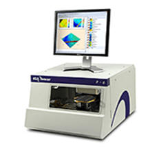
KLA-Tencor P-6 Surface Profiler |
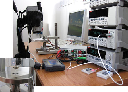
4-point probe
|
Oriel class AAA solar simulator
|
|
Surface analysis system
- Step heights and surface roughness
- Stress of thin films
- Surface roughness, waviness, peak count distribution and
more than 40 surface parameters
- 3D imaging of any area measured
Specifications:
- Vertical range up to 1 mm
- Scan length 150mm
- Applied load 05-50 mg
- Vibration-isolating workstation
|
- Measurement of low and high resistivity of thin films and
bulk materials
- Determination of the type of conductivity of semiconductors
|
- Measurement of current-voltage characteristics of solar cells
- Spectral range 400 – 1100nm
- Determination of solar cell parameters:
- Open circuit voltage (Voc)
- Short-circuit current (Isc)
- Current density (Jsc)
- Fill factor (FF)
- Solar cell efficiency (μ)
- Maximum output power (Pmax)
- Uniform and collimated light on an area 100x100mm
- Xenon arc lamp 450W
- 100mW/cm
- Filter AM 1,5 Global
- Meets the standards EIC 60904-9:2007 JIS C 8912, ASTM E927-05
|
Nanoindentation and tribology
 |
 |
|
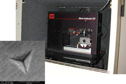
NanoIndenter XP with CSM module
|
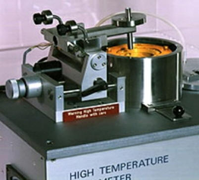
High Temperature Tribometer CSEM
|
|
Specifications:
- Continuous Stiffness Measurement - CSM
- Displacement resolution <0.01 nm
- Total Indenter travel 2 mm
- Maximum indentation depth >500 μm
- Max. load with high-load option 10 N (1 kg)
- Load resolution 50 nN (5.1 μgm)
- Contact force <1.0 μN
- Positioning accuracy 1.5 μm
- Video screen 25X
- Objective 10X & 40X & 100X
Possibilities:
- Superior means of nanomechanical characterization
- Full characterization of film – substrate interactions
- Hardness and modulus as a function of depth (CSM)
- Creep measurement
- Microscratch test
- Profilometry
|
Specifications:
- Pin-on-disc method
- Precisely calibrated friction and wear measurements at
elevated temperatures up to 800°C
- Efficient heating/cooling system to accurately maintain
desired test temperature
- High thermal stability
- Automatic shut-off at selected track length or friction
coefficient threshold
- Powerful software package for PC-controlled data acquisition
and instrument control
Possibilities:
- Simulate in-service conditions up to 800°C
|
|